High Frequency PCB Manufacturing: Key Considerations for Reliable High-Speed Electronics
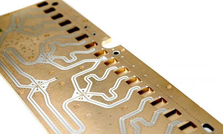
As electronic systems continue to operate at higher speeds and frequencies, PCB design and manufacturing become increasingly sensitive to small physical variations. In conventional boards, a minor change in trace geometry or layer construction may have limited impact. In high-speed applications, however, the same variation can affect signal integrity, impedance, timing, and overall system performance.
This is why high frequency PCB manufacturing requires closer coordination between PCB designers and manufacturers. The objective is not simply to fabricate a board according to a set of drawings, but to maintain the electrical characteristics defined during the design stage through controlled manufacturing.
Why High-Frequency PCB Design Requires More Control
High-frequency signals are strongly influenced by the physical structure of the PCB. Several factors can affect electrical behavior, including:
- Trace width and spacing
- Dielectric thickness
- Copper geometry
- Layer arrangement
- Manufacturing tolerances
A PCB stack-up is therefore an important part of the overall design. The position of signal layers relative to reference planes can influence impedance and routing behavior. Changes in dielectric thickness can also affect the relationship between a trace and its reference plane.
For this reason, high-frequency designs should not treat PCB fabrication as a separate step that begins after engineering work is complete. Manufacturing capabilities and tolerances should be considered while the stack-up and routing strategy are still being developed.
Stack-Up and Dielectric Thickness
The stack-up defines how the different conductive and insulating layers are arranged inside the PCB. For high-speed applications, this structure must support controlled routing while providing predictable electrical characteristics.
Dielectric thickness is particularly important because the distance between a signal trace and its reference plane affects impedance. If the actual manufactured thickness differs significantly from the design target, the resulting impedance can also change.
A well-planned stack-up should consider these factors together:
- Signal layers
- Reference planes
- Dielectric thickness
- Copper characteristics
- Available manufacturing tolerances
Early stack-up review can identify potential problems before fabrication and reduce the risk of repeated prototype revisions.
Multilayer construction can also help engineers organize high-density designs. FastTurnPCB supports PCB manufacturing of up to 50 layers, giving designers flexibility when complex routing, multiple reference planes, or high signal density are required.
Trace Width, Spacing, and Signal Integrity
Trace geometry is another critical factor in high-frequency PCB manufacturing. Trace width directly influences impedance, while spacing between traces can affect coupling and interference.
When signals are routed close together, unwanted electromagnetic interaction can become a concern. Designers therefore need to consider not only whether a trace can physically fit on the board, but also whether its width and spacing are appropriate for the intended electrical performance.
Manufacturing capability matters because the finished trace must remain within the dimensional limits specified by the design. FastTurnPCB supports minimum line width and spacing down to 2.5/2.5 mil, providing flexibility for dense and demanding PCB layouts.
However, smaller geometry also increases the importance of manufacturing consistency. A design that depends on tightly controlled trace dimensions requires a manufacturing process capable of repeatedly producing those dimensions.
Controlled Impedance and Manufacturing Consistency
Controlled impedance is essential when signals must travel between components with predictable electrical behavior. The target impedance is influenced by several physical factors:
- Trace width
- Trace spacing
- Dielectric thickness
- Layer structure
- Reference-plane configuration
Early communication between the design team and manufacturer is especially valuable. If a proposed stack-up or routing arrangement creates manufacturing challenges, those issues can be addressed before boards are fabricated.
For demanding applications, Fast Turn PCB manufacturing can support controlled impedance with a stated ±5% impedance tolerance. The company also provides stack-up optimization and DFM support to help engineers align PCB designs with manufacturing requirements.
Manufacturing consistency is equally important when multiple prototypes or production batches are required. Maintaining similar trace dimensions, layer alignment, dielectric construction, and other physical parameters helps ensure that different board revisions behave consistently.
Manufacturing Tolerances in High-Frequency Boards
High-frequency performance depends on more than the nominal values shown in a PCB design file. Real manufacturing processes involve tolerances, and those tolerances must be considered during engineering.
Variations in the following areas can influence impedance and signal behavior:
- Trace width
- Trace spacing
- Dielectric thickness
- Layer alignment
If these variations are not considered early, a board may require additional design iterations after testing.
A capable manufacturer should therefore understand the relationship between design specifications and fabrication limits. DFM review can help identify areas where the design may need adjustment while changes are still relatively easy to make.
FastTurnPCB provides engineering support for stack-up optimization, impedance control, and DFM. This coordination allows engineers to evaluate manufacturability before committing to production and can help reduce avoidable prototype problems.
Applications in 5G, Networking, and RF Systems
The importance of high-frequency PCB control is particularly visible in communication and RF equipment. Modern routers and switches must support increasingly high data rates, while 5G and emerging 6G systems place demanding requirements on signal transmission.
Antenna systems and RF equipment can also require carefully controlled PCB structures because unwanted signal loss, reflections, or interference may affect overall system behavior.
Common applications include:
- 5G and 6G equipment
- Routers and network switches
- Antenna systems
- RF equipment
- High-speed communication systems
In these applications, the PCB is part of the electrical system rather than simply a mechanical platform for mounting components. The stack-up, trace geometry, impedance, and manufacturing consistency can all contribute to final equipment performance.
Designing with Manufacturing in Mind
One of the most effective approaches to high-frequency PCB development is to involve the manufacturer early. Instead of completing the entire layout and then checking whether it can be fabricated, designers can review manufacturing constraints while developing the stack-up and routing strategy.
This approach can help engineers make informed decisions about:
- Trace width and spacing
- Layer arrangement
- Dielectric thickness
- Impedance requirements
- Manufacturing tolerances
It can also reduce the likelihood of discovering fabrication limitations after a prototype has already been produced.
For complex multilayer boards, the manufacturer’s ability to support advanced structures and maintain dimensional consistency becomes especially important. FastTurnPCB combines multilayer manufacturing capability with engineering assistance, helping designers connect electrical requirements with practical fabrication considerations.
Conclusion
Reliable high-frequency PCB performance depends on the relationship between electrical design and manufacturing precision. Stack-up configuration, dielectric thickness, trace width and spacing, impedance requirements, and manufacturing tolerances all need to be considered together.
For 5G and 6G equipment, routers, switches, antennas, and other communication or RF systems, early design-to-manufacturing coordination can help prevent avoidable signal-integrity problems.
Key manufacturing capabilities include:
- Up to 50-layer PCB manufacturing
- 2.5/2.5 mil minimum line width and spacing
- ±5% impedance tolerance
- Stack-up optimization
- DFM engineering support
Ultimately, successful high-frequency PCB development begins before fabrication. When designers and manufacturers work together from the stack-up and routing stages, the result is a more controlled development process and a stronger foundation for reliable high-speed electronics.